

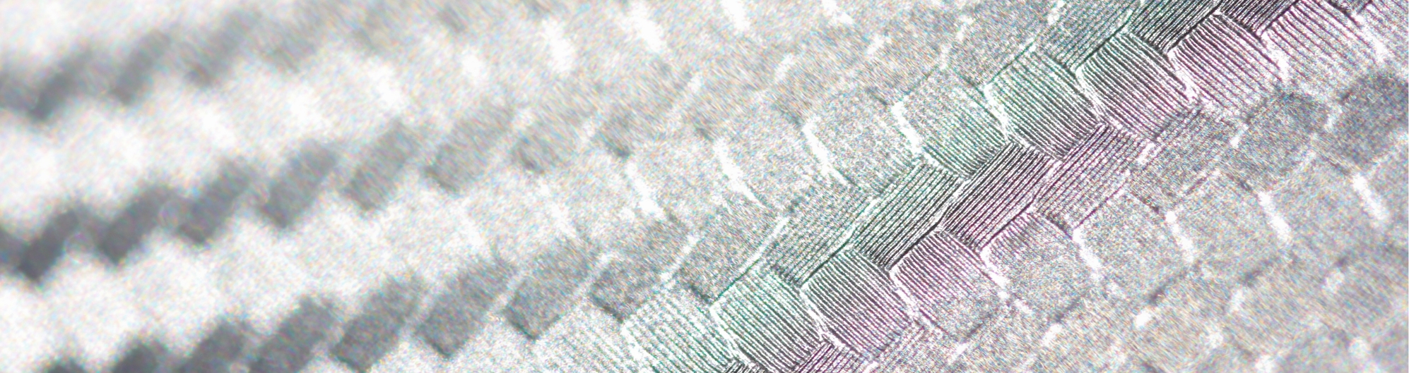

2D ENGINE consortium has realized ultrathin layers of semiconductor and dielectric materials
2D ENGINE consortium has realized ultrathin layers of semiconductor and dielectric
materials using liquid metal catalyst growth, greatly assisted by in-situ, real time
monitoring tools developed partly within the project.
SUMMARY OF THE PROJECT AND MAIN RESULTS
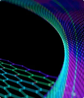
The 2D ENGINE project looks for 2D semiconductor and dielectric materials which cannot be exfoliated from bulk but they need to be engineered as atomically thin films using chemical vapor deposition on metal catalyst substrates or on melted surfaces. The semiconducting materials are envisaged to have the outstanding stability of graphene and offer excellent electrostatic control in digital electronic devices which allows their miniaturization and their operation with superb energy efficiency. The project mobilizes diverse expertise in materials science and engineering, materials growth, condensed matter physics, atomistic simulation, in-situ surface characterization techniques, equipment development, semiconductor processing and electrical engineering to face the challenges.
We envision that our atomically thin semiconductor channels combined with ultrathin dielectrics, will form the next generation of the multisheet gate-all-around field effect transistor (GAAFET) architectures. It is expected that the 2D ENGINE devices will have an impact on the efforts for chip miniaturization according to the requirements of future aggressively scaled 2 nm technology nodes. Moreover, 2D ENGINE targets the integration of 2D light emitting diode (LED) devices with planar waveguides to increase the efficiency of silicon photonic integrated circuits (PIC) for low power on-chip communications.
The envisaged free-standing wafer scale 2D semiconductors and dielectrics are expected to be transferable so they could offer innovative solutions for the integration of power devices on the back-side of the wafer with the aim to decouple the power delivery network from the signal (logic) network on the front side of the wafer.