
Context and overall project objectives
The 2D ENGINE project looks for 2D semiconductor and dielectric materials which cannot be exfoliated from bulk but they need to be engineered as atomically thin films using chemical vapor deposition on metal catalyst substrates or on melted surfaces. The semiconducting materials are envisaged to have the outstanding stability of graphene and offer excellent electrostatic control in digital electronic devices which allows their miniaturization and their operation with superb energy efficiency. The project mobilizes diverse expertise in materials science and engineering, materials growth, condensed matter physics, atomistic simulation, in-situ surface characterization techniques, equipment development, semiconductor processing and electrical engineering to face the challenges.
We envision that our atomically thin semiconductor channels combined with ultrathin dielectrics, will form the next generation of the multisheet gate-all-around field effect transistor (GAAFET) architectures. It is expected that the 2D ENGINE devices will have an impact on the efforts for chip miniaturization according to the requirements of future aggressively scaled 2 nm technology nodes. Moreover, 2D ENGINE targets the integration of 2D light emitting diode (LED) devices with planar waveguides to increase the efficiency of silicon photonic integrated circuits (PIC) for low power on-chip communications.
The envisaged free-standing wafer scale 2D semiconductors and dielectrics are expected to be transferable so they could offer innovative solutions for the integration of power devices on the back-side of the wafer with the aim to decouple the power delivery network from the signal (logic) network on the front side of the wafer.
Work performed and main achievements
The main objective for the first 18-month period was to develop ultrathin 2D semiconductor and dielectric/insulating layers of sufficient quality that could be used for the fabrication of thin channel FETs and thin active layer LEDs in the project periods to follow. In more detail, the consortium focused on obtaining good quality ultrathin films with good surface coverage at a wafer scale and validated them in terms of structural and morphological integrity and stability to ensure that electronic grade materials are obtained for device fabrication. Moreover, the consortium adapted layer transfer methodologies known from graphene research to develop new layer transfer protocols from the growth to the target substrates, an important task towards devices fabrication
The work on different materials was distributed among different partners for best efficiency. NCSRD worked on graphitic h-SiC, U. Patras in collaboration with LPM, ULEI, and ESRF on h-BN, ESRF in collaboration with ULEI on h-GaN. For all materials, the partners used Liquid Metal Catalyst (LMCat)-based methodology with the necessary adaptations specific to the material under investigation. AMO worked with all partners preparing appropriate test substrates for the evaluation of their electrical properties. In addition, MPG collaborated with growers and materials process developers to structurally characterize grown materials using both, atomistic simulations to produce reference data and (AI-guided) computer vision to establish an automated analysis of recorded images and spectra.
2D ENGINE made significant progress in all materials classes mentioned above, also made important accomplishments which can be headlined as follows:
(a) We have obtained compelling evidence that cm-scale thin SiC membrane is catalytically grown on melted Silicon surfaces by CVD
(b) Large area ultrathin (3-4 mL) GaN has been grown, in-situ monitored by Radiation Mode Optical Microscopy (RROM) at a reactor located in the synchrotron facility. In addition, thin GaN crystals with good surface coverage were obtained in different reactor
(c) ![]()
![]() Multilayer and ultrathin crystals of 2D h-BN have been achieved by LMCat. The growth has benefited from real-time RMOM as well as from improvements in the reactor, which are implemented within the project.
Multilayer and ultrathin crystals of 2D h-BN have been achieved by LMCat. The growth has benefited from real-time RMOM as well as from improvements in the reactor, which are implemented within the project.
(d) h-BN and graphene were successfully transferred from LMCat growth substrates onto SiO2/Si target substrates and characterized to verify their morphological integrity.
(e) Automated analysis of experimental RMOM and Raman spectra as well as real-time experimental control via computer vision have been demonstrated
Results beyond the state of the art
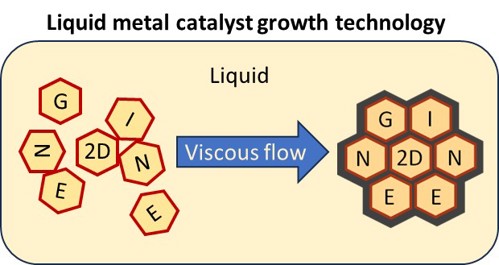
The project has achieved significant intermediate results which help a lot achieving our final goals. Atomically thin 2D semiconductors (SiC, GaN) and dielectrics (h-BN) have been obtained. These are the main ingredients of future aggressively scaled digital electronic devices with good electrostatic control and low leakage currents. The materials are in the form of wafer scale free-standing 2D thin film layers which are transferable. This provides flexibility in their integration with silicon devices and circuits and presents an advancement beyond the state of the art. Equally important is the method used to produce the ultrathin materials which is based on chemical vapor deposition (CVD) on liquid metal catalyst (LMCat) substrates or on melted surfaces. This technique of growing 2D materials is an innovative methodology beyond the state of the art. It suggests growth on melted surfaces with viscous flow instead of the typically used rigid (solid) substrates and is a paradigm shift for the growth of 2D materials, in general.
The already grown innovative 2D materials require further validation of their crystallographic structure, their stability in air and under thermal and chemical treatment before they are used to devices. Layer transfer has already been developed but it needs to be perfected. All the aforementioned improvements will be done based on project's resources. After the project end we foresee the valorization of our materials and technology in a pilot line, most likely the 2D PL pilot operating within the Graphene Flagship initiative in a time frame of 2 to 3 years. The main aim is to find out whether the new 2D materials can be processed using standard semiconductor manufacturing equipment and conclude whether new in-line and end-of-line inspection tools are needed. The most challenging will be to validate the suitability liquid metal catalyst (LMcat) growth technology with pilot lines. Cross contamination issues and cleaning of equipment methods must be addressed. While valorization of or materials and technologies is a first step, more steps are needed for commercialization. Further validation in development at higher TRL requires validation in advanced pilot lines such as the ones run by CHIPS JU and transfer of the LMCat technology to large area wafers (8 or 12 inch) in a timeframe of 3-5 years.
Project contributions to the research policies
The project is expected to have an impact on chip miniaturization to address the needs of aggressively scaled (2 nm) technology node. In addition, the project aims to improve the efficiency of Si photonic integrated circuits with a possibility to also have a contribution to quantum photonic circuits. As such, the project results could influence the Chips Act initiative of the EU especially at the level of drafting new calls that would take into account new (2D) semiconductor materials. The new materials are compatible with Si processing, therefore they show prospects of being manufacturable and offer potentially enhanced performance and flexibility when integrated with Si devices and circuits. Chips JU policies could include new Si compatible 2D materials and validate their potential for volume production using one of the already established pilot lines.
On the other hand, the 2D ENGINE results could help shaping the SRIA of the newly formed IAM-I initiative on innovative advanced materials and help with drafting new Calls. 2D ENGINE is part of the Graphene flagship initiative, one of the main components of IAM-I, therefore, channeling of information and knowledge from 2D ENGINE to the IAM-I working groups and task forces is facilitated. As a result, we expect an influence of our project on the EU policies on advanced materials.
Image 1
Image 2